 EN
EN CN
CN JP
JP


Solar wafer contour positioning
Solar wafer contour positioning
Application description
Visually photograph the outline of the silicon wafer, locate the center and angle of the product, and check whether the edge of the silicon wafer is damaged.
Accuracy requirement: 0.05mm, field of view size: 250 * 180mm.

Original Image
|
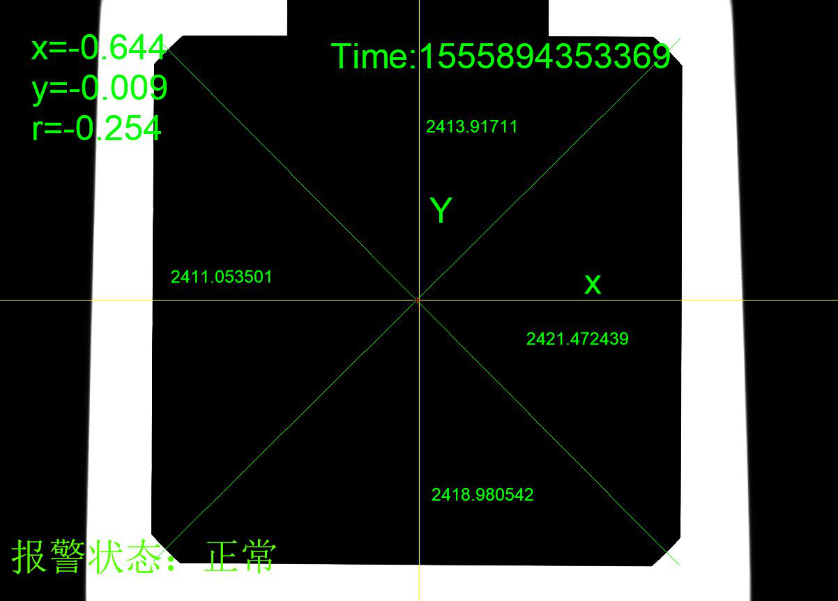
Result Image
|
|
- Contact OPT:
- Contact Sales Team|
- Get Product Demo|
- Get Product Quote


